Observation Examples of Thin Film
Observation of the surface topography and current distribution images of a P3HT and PCBM blended film
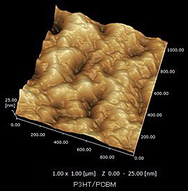
Figure 1: surface topography
Figure 2: current distribution image
observed under dark (upper half)
and under illumination (lower half)
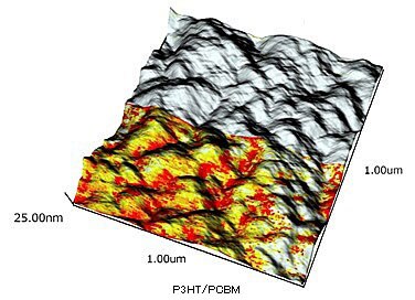
Figure 3: 3D plot of the film topography overlaid with the current distribution
P3HT and PCBM are widely-used semiconducting materials for polymer-based solar cells. Here, the surface topography and current distribution were imaged for the blended film of P3HT and PCBM, which acts as a photoactive layer of the solar cells.
The P3HT/PCBM blended film (1:1 wt ratio) was spin-coated onto a transparent electrode.
To characterize the optoelectronic property at nanometer scale, the AFM imaging was performed for the blended film under the illumination of 532-nm light. Figure 1 and 2 shows the topographical and current distribution images, respectively: the upper half of these images was obtained under dark and the lower half was under illumination. As shown in Figure 2, the photocurrent (maximum 10 pA) was observed under illumination, while the topographical image collected simultaneously was not changed. The photocurrent image represents the charge-carrier generation in the P3HT/PCBM blended film.
Figure 3 shows a 3D plot of the film topography overlaid with the current distribution, which depicts the correlation between the topography and local photocurrent response.
P3HT: regioregular poly(3-hexylthiophene)
PCBM: [6,6]-phenyl-C61-butyric acid methyl ester
(Courtesy of Assistant Prof. Hiroaki BENTEN, Graduate School of Engineering, Kyoto University)