Observation Examples of Nanotechnology
Drawing by Potential
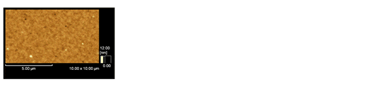
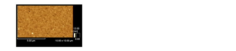
Drawing of tracks as shown in Fig.1 was done by the vector scanning on a Au sample deposited on silicon substrate. At this time, minute potential was given by using an conductive cantilever between the sample and the cantilever. After drawing, AFM and KFM were measured simultaneously. Then, the potential of tracks of drawing was measured about 50mV lower than surroundings in the potential measurement of the KFM image (Fig.3), though the change was not admitted in the shape observation of the AFM image (Fig.2).
(Data provided by Prof. Hasegawa and Dr. Eguchi, The Institute for Solid State Physics, The University of Tokyo)