Observation Examples of Thin Film
Observation of ITO Thin Film
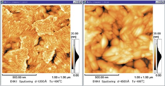
The surface topography of ITO thin film, which is known as a transparent, conductive film, varies with the deposition technique, the film thickness, the substrate temperature, and other deposition conditions. By comparing ITO thin films of thicknesses 120 nm (left) and 450 nm (right), it can be clearly seen that, with increased film thickness, the individual crystal grains grow bigger. The grain–sub-grain structure peculiar to the sputtering method can also be observed.
(Data provided by Dr. Shigesato, Department of Chemistry, College of Science and Engineering, Aoyama Gakuin University)