3D-DIC Analysis in Impact Test
TOPICS
Overview of Shimadzu’s Online
Ultrapure Water Measuring Technology
TOPICS
Overview of Shimadzu’s Online
Ultrapure Water Measuring Technology
Ultrapure Water is Important for the Semiconductor Industry
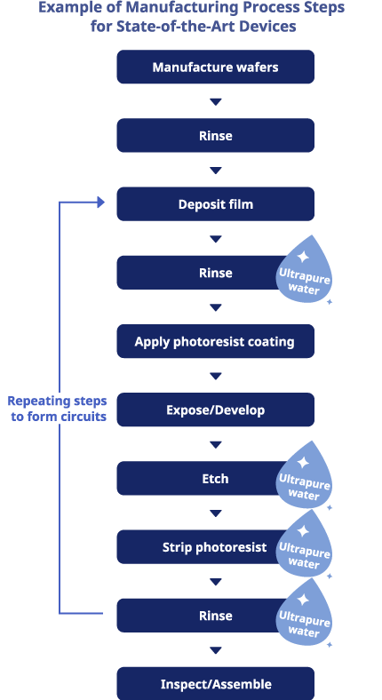
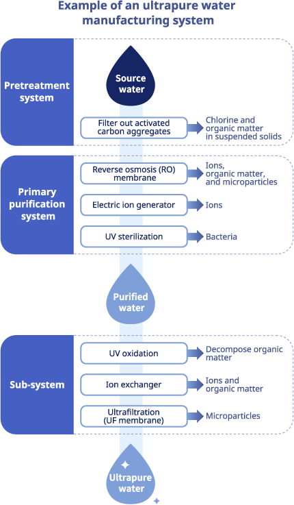
Large volumes of ultrapure water are used to manufacture semiconductors, particularly for rinsing processes. With increasing miniaturization of semiconductors, even ultra-trace quantities of impurities or organic matter can cause defects or lower yield. Therefore, maintaining the high purity of ultrapure water is essential for quality and reliability. Typically, a conductivity of 18.2 MΩ and a TOC (total organic carbon) level below 1 ppb are required to ensure a reliable supply of high-purity/ultrapure water. This is an essential prerequisite for ensuring the reliability of semiconductor devices.
![]()
Required
Online Ultrapure Water Measurements
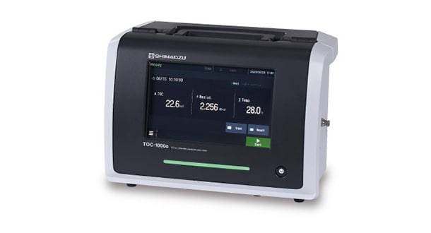
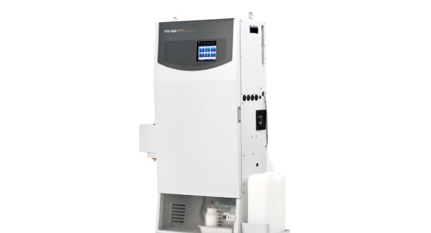
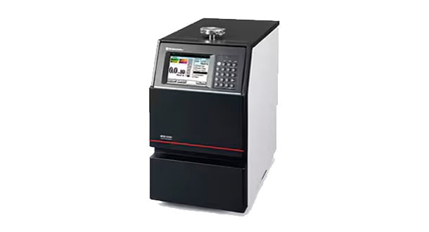
TOC-1000e S
On-Line TOC Analyzer for Pure Water
In semiconductor manufacturing, even the smallest trace of contamination can compromise product quality. As semiconductor miniaturization continues to advance, minimizing trace-level organic contamination has become increasingly critical to maintain high product yield rate. As a result, the quality standards for ultrapure water used in semiconductor manufacturing are becoming even stricter. Especially in the manufacturing process of cutting-edge semiconductors, the need to detect urea and other hard-to-oxidize compounds has increased. Detecting those compounds has been difficult using conventional techniques. The TOC-1000e S on-line TOC analyzer for ultrapure water, incorporating feedback from cutting-edge semiconductor manufacturers, has been developed to address these challenges.
Learn More

APPLICATION

01
For Semiconductor
Devices
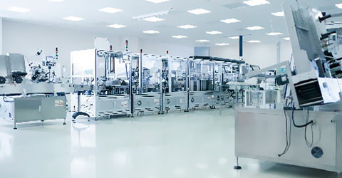
Due to advancements in the miniaturization and circuit integration of semiconductor devices, quality requirements for materials manufacturing environments have become much stricter. The factors that affect device performance and yield include water purity, gas purity, the cleanroom environment, and mounting quality. As a result, a wide variety of analytical and evaluation technologies are employed in the manufacturing process to evaluate organic matter in ultrapure water, analyze pollutants in the air, monitor hazardous chemical substances, check the purity of processing gases, conduct non-destructive inspection to ensure the reliability of device mounting operations, and so on.
-
Online TOC Measurement for Ultra-pure Water in Semiconductor Industries
The semiconductor manufacturing process involves various stages such as wafer production, film formation, photolithography, etching, and resist stripping, each of which involves cleaning steps. Even minimal contamination on the semiconductor surface can impact product quality and yield, making it crucial to effectively remove dirt and impurities during cleaning. For this reason, the purity of the cleaning water used in these cleaning processes is extremely important.
Learn More
-
Evaluation of TOC in Source Water, Recovered Water, and Effluent
Due to the large volumes of water used at semiconductor manufacturing plants, it is essential to utilize water resources efficiently and reduce environmental impacts. Source water is evaluated based on determining the organic matter load and pretreatment efficiency, which are useful for deciding whether or not recovered water can be reused. For effluent water, TOC measurements are used to ensure compliance with environmental regulations or to confirm that treatment facilities are operating smoothly.
Learn More
-

Simultaneous Analysis of Multiple PFAS Components in Effluent Water
Given the increasingly strict PFAS (organofluorine substance) regulatory requirements in recent years, there is an increasing probability that PFASs are detected in effluents from semiconductor manufacturing operations. Triple quadrupole LCMS systems can quantitatively analyze multiple PFAS types simultaneously, making them an essential tool for reducing environmental impact and ensuring regulatory compliance. Monitoring PFAS compounds in effluent water from ongoing operations is also important from the perspective of both social responsibility and business sustainability.
Learn More
-
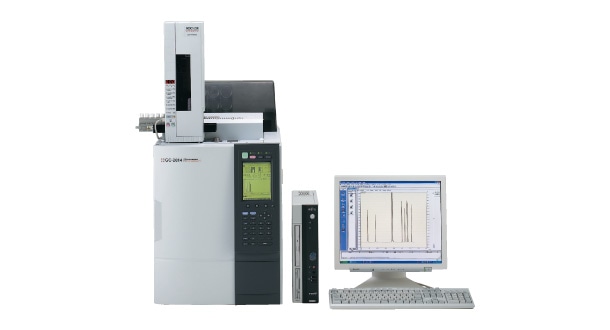
Analyzing Impurities in Gases
High-purity gases (bulk gases and various specialty gases) are used in semiconductor manufacturing processes. Impurities in these gases can directly affect yield rates and device reliability, so gas impurity levels must be monitored. By automating processes ranging from sampling to data acquisition and output, GC systems provide stable, long-term performance and enable the high accuracy, high sensitivity, and high separation analysis of gas purity.
Learn More
-
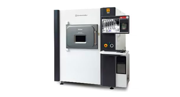
Evaluating Device Mounting Reliability by Non-Destructive X-Ray Inspection
Completed semiconductor devices are assembled into the final electronic product only after undergoing a mounting process. Voids, bridges, cracks, or other defects in solder joints used during those processes can decrease reliability. Non-destructive X-ray inspections allow internal structures to be observed without damaging them, with external inspections used to detect complex microdefects. This ensures higher mounting quality, improves yield rates, and enables faster defect analysis.
Learn More
-
Analyzing Air Quality in Clean Rooms
Due to the miniaturization of semiconductors, not only inorganic microparticles but also organic compounds generated from clean room materials, device manufacturing equipment, and human bodies increasingly need to be controlled for semiconductor manufacturing processes.

02
For Semiconductor Manufacturing Equipment
Due to the increasing miniaturization and higher integration of semiconductor devices, performance requirements for semiconductor manufacturing equipment have increased significantly. In particular, maintaining a clean and consistent processing environment, using more advanced vacuum technologies, and ensuring airtightness are essential factors that can affect yield rates and reliability. Precision control technologies and sophisticated detection technologies have been introduced to achieve stable equipment operation and high throughput, which form the foundation for advances in the semiconductor industry.
-
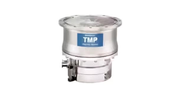
Improved Evacuation Pumping Performance of Semiconductor Manufacturing Equipment
Optimizing gas evacuation systems enables process gases to be evacuated at high flowrates, which achieves lower process chamber pressures. The temperature control (heating) system and a feature that prevents process gases from flowing back to mechanical areas help extend turbomolecular pump service life and reduce running costs.
Learn More
-
Maintenance of Semiconductor Manufacturing Equipment
A leak detector equipped with a 270-degree polarized analysis cell enables high-precision and high-efficiency maintenance of semiconductor manufacturing equipment. Available as dry-type models for use in clean rooms, and as mobile models that can be freely moved around the factory. Various optional products are also available. Featuring hydrogen/helium dual-use specifications, the product lineup, which is manufactured in Japan and backed by an extensive service network, ensures safe and worry-free operation.
Learn More
SOLUTION
Applications for each manufacturing process are described below. Semiconductor manufacturing involves
photolithography, etching, film deposition, rinsing, inspecting, and other process steps.
Photolithography
is used to form the detailed circuit patterns and etching is used to remove unwanted material. Film deposition
is used to form thin films and rinsing keeps wafers clean. Inspection processes are used to check product
quality. Such processes are essential for improving semiconductor manufacturing efficiency and quality.
Wafer
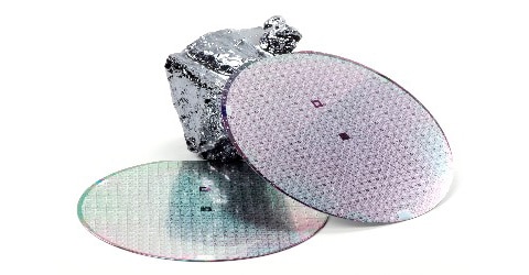
Wafers are an essential material in semiconductor manufacturing. In R&D and production processes, various analyses and evaluations such as band gap measurement and photoresist film thickness measurement are performed.
Others [Semiconductor]