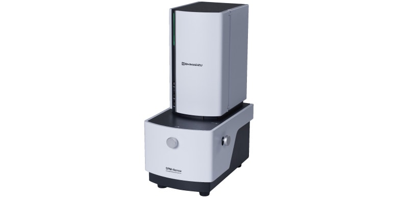
SPM-Nanoa
-� SPM enables observation of the piezoelectric response of individual polarization domains, which is a key factor determining the characteristics of piezoelectric materials. �- Evaluation based on an atmosphere (air, inert gas, low vacuum) close to the actual use environment is possible. �- Detailed searches for targets can be conducted with a high resolution optical microscope, which is integrated with the SPM in a single system.
Piezoelectric materials have the piezoelectric property that application of a voltage causes deformation. Utilizing this characteristic, these materials play an important role as sensors, buzzers, and filters in various industrial products. Recently, particularly with ongoing downsizing of electronic equipment and communication devices, even higher performance has been required in piezoelectric materials, and development is being promoted energetically. Piezoelectric materials are composed of aligned spontaneous polarization regions (domains). These domains are polarized in different directions and display different responses to applied voltage. The response of the individual domains is a key factor that determines the characteristics of a piezoelectric material. However, high sensitivity is required in order to evaluate the domain response because deformation on the nanometer order under an applied voltage is not uncommon. Here, we introduce an example in which the minute response of a piezoelectric material to an applied voltage was captured by using a scanning probe microscope (SPM (AFM)), which is capable of detecting the piezoelectric response at the sub-nanometer order.
May 6, 2021 GMT
