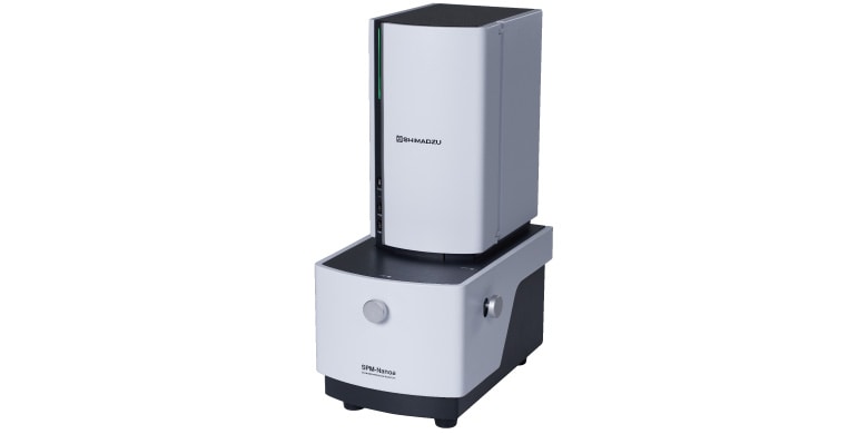
SPM-Nanoa
- The high performance optical microscope integrated into the SPM enables precise target location. - Accurate target capturing eliminates the need for rework in locating the field of view, realizing more efficient operations. - Patterned Si substrates can be easily observed without sample preparation.
Scanning Probe Microscope [SPM (AFM)] is a microscope that enables easy, high-resolution 3D observation at the nano meter scale in air. The range of application is extensive, from hard materials such as semiconductor substrates and metals to soft materials such as biological samples. As the miniaturization of electronic devices and bio-devices progresses, further miniaturization is required for the parts comprising these devices. For example, in the semiconductor industry, the line width of circuits used to be 10μm when integrated circuits were first developed, but now it is 14 nm. Due to such micronization of parts, the selection of locations to observe with microscopes is now required to be even more precise compared to the past. Since SPM has a high resolution and high magnification, it is necessary to strictly specify the observed location. Although an observed location for SPM is usually selected using an optical microscope, precise positioning has not conventionally been possible, due to the lack of resolution on the optical microscope. However, SPM-Nanoa integrates a high-performance optical microscope, thereby facilitating precise location of the target on the micrometer.
September 24, 2021 GMT
