Observation of the shape of ITO thin films
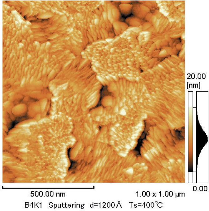
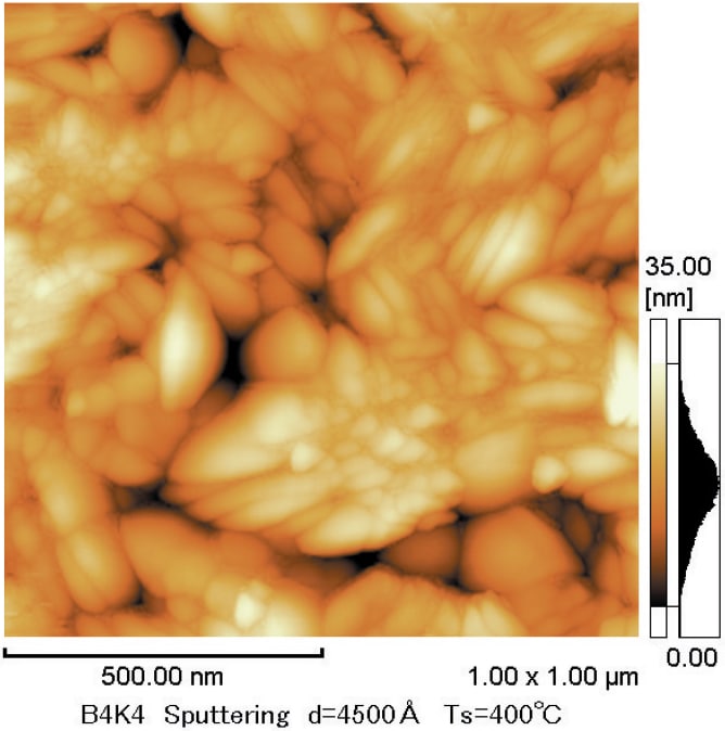
The surface shape of ITO thin films, which are known as transparent conductive films, varies depending on the deposition method, film thickness, substrate temperature, and other conditions. Comparing the ITO thin films with a film thickness of 120 nm (left) and 450 nm (right), it is clear that individual grains grow larger as the film thickness increases. In addition, the grain-subgrain structure peculiar to sputtering is clearly observed.
(Data provided by Dr. Shigesato, Department of Chemistry, Faculty of Science and Engineering, Aoyama Gakuin University)