AIRsight™ - Applications
Infrared/Raman Microscope

Most of the documents on the LITERATURE is available in PDF format. You will need Adobe Acrobat Reader to open and read PDF documents. If you do not already have Acrobat Reader, you can download it free at the Adobe's Website. Click the GET ADOBE READER icon on the left to download a free copy of Adobe Acrobat Reader.
Contaminant
Infrared Raman
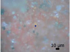
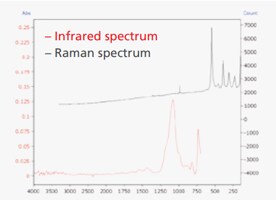
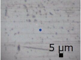
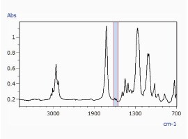
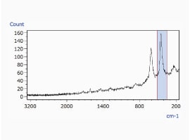
This is an example of analyzing a contaminant (simulated sample) attached to the surface of a pharmaceutical tablet. Obtaining both infrared and Raman measurements from the same spot increases the accuracy of qualitative analysis to help identify the cause of contaminants.
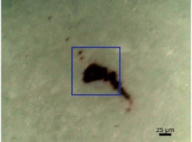
Microscope Image of Contaminant
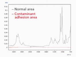
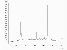
Infrared Spectra of Normal and Contaminant Adhesion Areas with Normal Area Identified as Mannitol
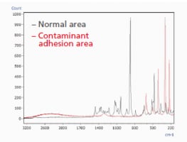
Raman Spectra of Normal and Contaminant Adhesion Areas with Contaminant Identified as Iron Oxide
Pigment
Infrared Raman
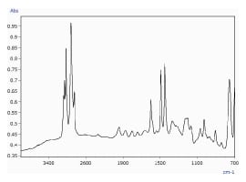
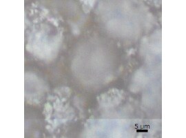
This is an example of analyzing pigment applied to wood.
Because AIRsight microscopes can measure trace quantities, they are especially useful for measuring precious samples with historical value.
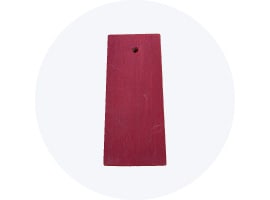
Appearance of Pigment Applied to Wood
Microscope Image of Pigment Applied to a
Wood Surface
Infrared and Raman Spectra of Pigment with
BaSO₄ Identified from the IR Spectrum and Pb₃O₄ from the Raman Spectrum
Microplastic
Infrared Raman
This is an example of analyzing a microplastic particle. The ability to measure infrared and Raman spectra from a wide range of microplastic particle sizes, from a few micrometers to several tens of micrometers in diameter, makes the system ideal for monitoring survey and research applications.
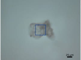
Image of Contaminant Microscope Image of Microplastic
Infrared Spectrum of 115 μm Long (Major Axis) and 53 μm Wide (Minor Axis) Microplastic Identified as Polystyrene
Microscope Image of Microbead
Raman Spectrum of 1 μm Diameter
Microbead Identified as Polystyrene
Carbon Material
Raman
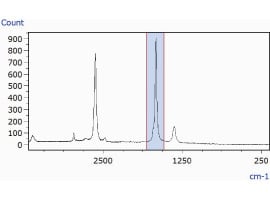
This is an example of analyzing a diamond-like carbon (DLC) film.
Raman measurements can determine bonds and structures in carbon materials with high sensitivity for use in the quality control of DLC films.
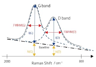
Diagram of Evaluation Parameters for Raman Spectrum of a DLC Film
| I(D)/I(G) Disturbances in Crystal Structure |
FWHM(G) Crystallinity, Young’s Modulus, and Density |
log(N(G)/I(G)) Hydrogen Concentration |
|
|---|---|---|---|
| CH4_center | 0.32 | 182.17 | -0.29 |
| CH4_periphery | 0.32 | 181.40 | -0.28 |
| C2H2_center | 0.34 | 190.85 | -0.44 |
| C2H2_periphery | 0.34 | 190.25 | -0.44 |
Results from Evaluating DLC Film (Formed with Either CH4 or C2H2 Gas) on Two Types of Silicon
Wafers (Measured in Two Locations—Near the Sample Center and Periphery)
Li-Ion Battery
Raman
This is an example of analyzing the negative electrode material from a lithium-ion battery.
Raman area mapping can be used to visualize the detailed distribution of components and structural characteristics in substances (crystallinity, defects, etc.). Therefore, it is useful for evaluating products and materials in R&D applications.
Note: In the chemical image shown, the red areas indicate high concentrations of the component and the blue areas indicate low concentrations.
Microscope Image of Negative Electrode Material
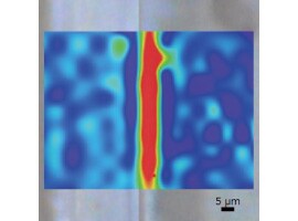
Raman Area Mapping Results Chemical Image of Graphite (G-Band)
Chemical Image Created from Peak Area Values between 1482 and 1703 cm-1
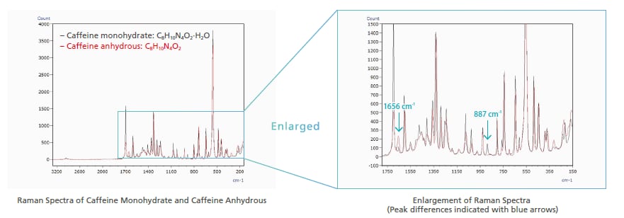
Polymorphic Crystal
Raman
This is an example of analyzing monohydrate and anhydrous forms of caffeine.
Raman spectra can differentiate between compounds that have identical chemical structures but with different crystal polymorphisms. Evaluating the crystal form of substances with different solubility or efficacy characteristics is useful for controlling crystal formation during pharmaceutical manufacturing processes.
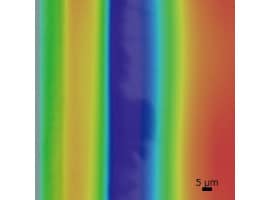
Multilayer Film
Infrared Raman
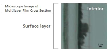
This is an example of analyzing a multilayer film.
The distribution of each component can be visualized by using infrared and Raman area mapping to analyze a cut cross-section from the film.
Infrared Area Mapping Results Chemical Image of Phthalate Esters
Chemical Image Created from Peak Areas between 1551 and 1624 cm-1
Raman Area Mapping Results Chemical Image of Titanium Oxide (Rutile)
Chemical Image Created from Peak Area Values between 345 and 508 cm-1
Automotive Paint Coating
Raman
This is an example of analyzing an automotive paint coating. Samples with characteristics that make it difficult to cut a cross-section can be evaluated by analyzing the component distribution in the depth direction by Raman spectroscopy and evaluating the degradation status or other criteria from the surface.
A separate mapping program (P/N 206-35093-41) is required.
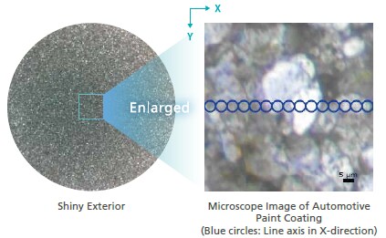
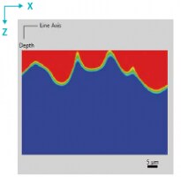
Raman Depth (Line) Mapping Results Chemical Image of Acrylic Resin
Chemical Image Created from Peak Area Values between 1383 and 1510 cm-1