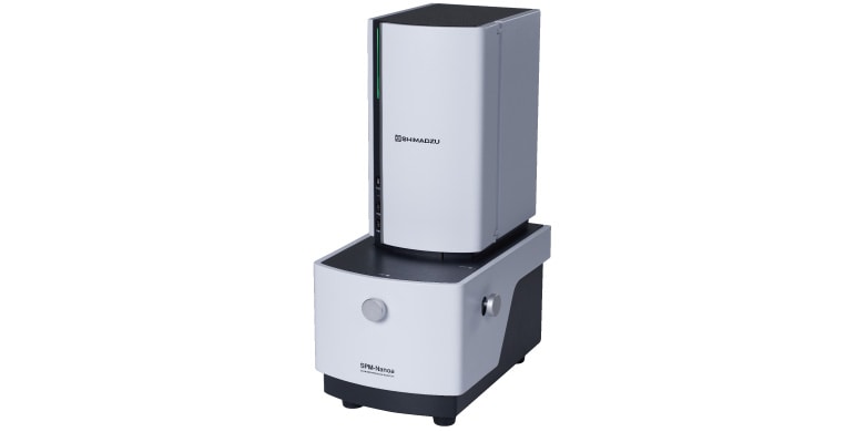
SPM-Nanoa
- With a single 8K high pixel observation, it is possible to check the 3D topography of a wide range and the detailed structure at any given point. - There is no need to reacquire data even when checking multiple regions. - Patterned substrates can be easily observed and analyzed without the need for pretreatment.
Scanning Probe Microscope [SPM (AFM)] is a microscope that enables easy, high-resolution 3D observation at the nano meter scale in air. The range of application is extensive, from hard materials such as semiconductor substrates and metals to soft materials such as biological samples. As the miniaturization of electronic devices and bio-devices progresses, further miniaturization is required for the parts comprising these devices. For example, in the semiconductor industry, the line width of circuits used to be 10μm when integrated circuits were first developed, but now it is 14 nm. Even so, since the number of pixels in the conventional SPM was only about 2K (2048 × 2048), it has been necessary to perform measurements at each location when multiple locations were to be observed in detail. On the other hand, SPM-Nanoa, which realizes 8K high pixel observation, can cut out a clear narrow image from a wide image, thus enabling us to observe the detailed structure of multiple locations in a single measurement. In this article, we introduce an example of 8K (8192 × 8192) high pixel observation on a patterned Si substrate.
September 24, 2021 GMT