Evaluation of Silver Sintered Die Attach Materials for Next-Generation Power Semiconductor Bonding
In recent years, the focus around next-generation mobility technologies, such as electric vehicles (EVs), has been to overcome technical challenges that limit driving range. Key priorities include minimizing energy loss, reducing weight and size, and improving voltage resistance. Of particular importance, inverters that handle large amounts of power require better conversion efficiency. To address these issues, efforts are underway to replace conventional Si power semiconductor element materials with wide bandgap semiconductors, such as SiC and GaN.
However, with increased output and density, the heat density also increases, and solder lacks the resistance to handle this increased heat. Silver and copper sintered materials (such as silver paste) are emerging as promising alternatives, with companies competing to develop them.
Fig. 2 illustrated the process by which a power semiconductor chip is mounted. The original materials (silver powder, solvent, dispersant, etc.) are made into a paste and printed onto the substrate. Then the chip is mounted and sintered by applying heat and pressure. Because the optimum sintering conditions vary depending on the material properties of the silver paste, evaluation of each process is necessary. This page introduces examples of evaluating silver paste, one of the power semiconductor bonding materials used in this new bonding technology.
-
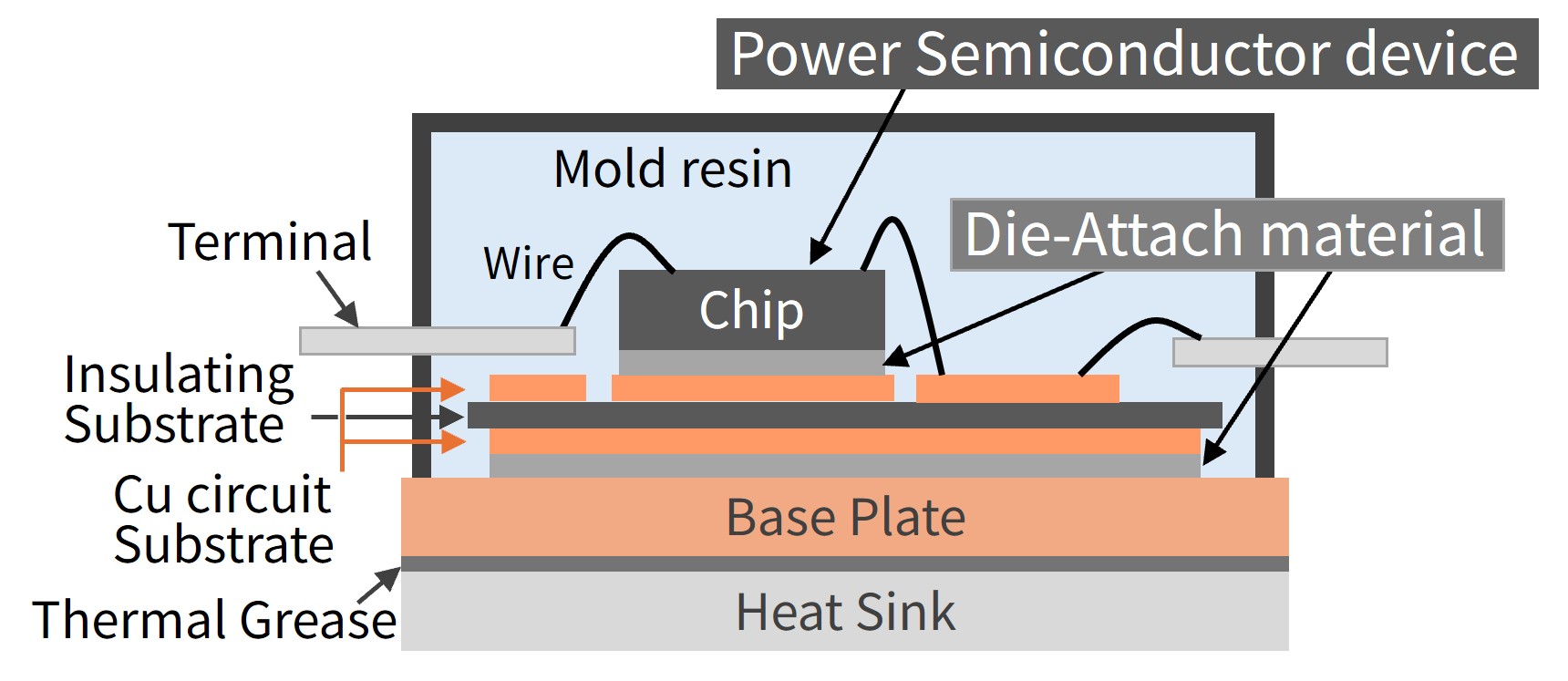
Fig. 1 Schematic Diagram of Power Semiconductor
-
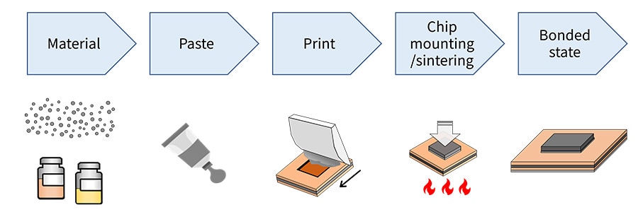
Fig. 2 Process of Mounting a Chip Using Power Semiconductor Die Attach Material (Silver Paste)
1. Evaluation of Particle Size of Sintering Material and Dispersibility of Paste
Evaluating the size and shape of the silver particle raw material and the dispersibility of the paste state when a solvent or dispersant is added serves as a vital function for selecting raw materials, maintaining consistent quality between lots, and analyzing bonding defects, etc.
Fig. 3 shows data from measuring the particle size distribution of each lot of raw powder using a laser diffraction particle size analyzer (SALD-7500nano). The properties of the raw material particles can be controlled using the particle size distribution of the raw material powders, from nanometers to micrometers.
To obtain more details, a dynamic particle image analysis system (iSpect DIA-10) was used to measure the size and shape of coarse particles in each lot of raw powder (Figs. 4 and 5).
Results show differences in the number of particles larger than a few μm between lots of the same product. In addition, the iSpect DIA-10 identified the shape of each individual detected particle.
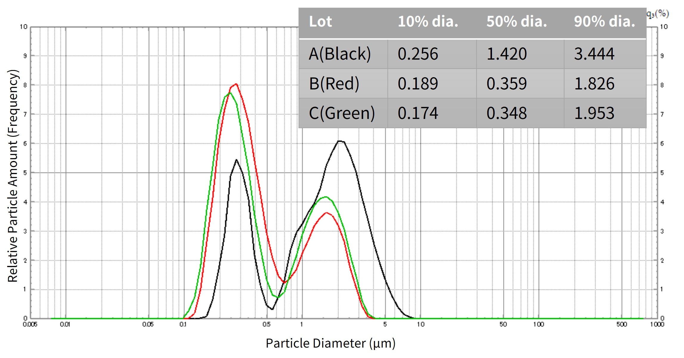
Fig. 3 Differences in Particle Size Distribution between Raw Material Powder Lots
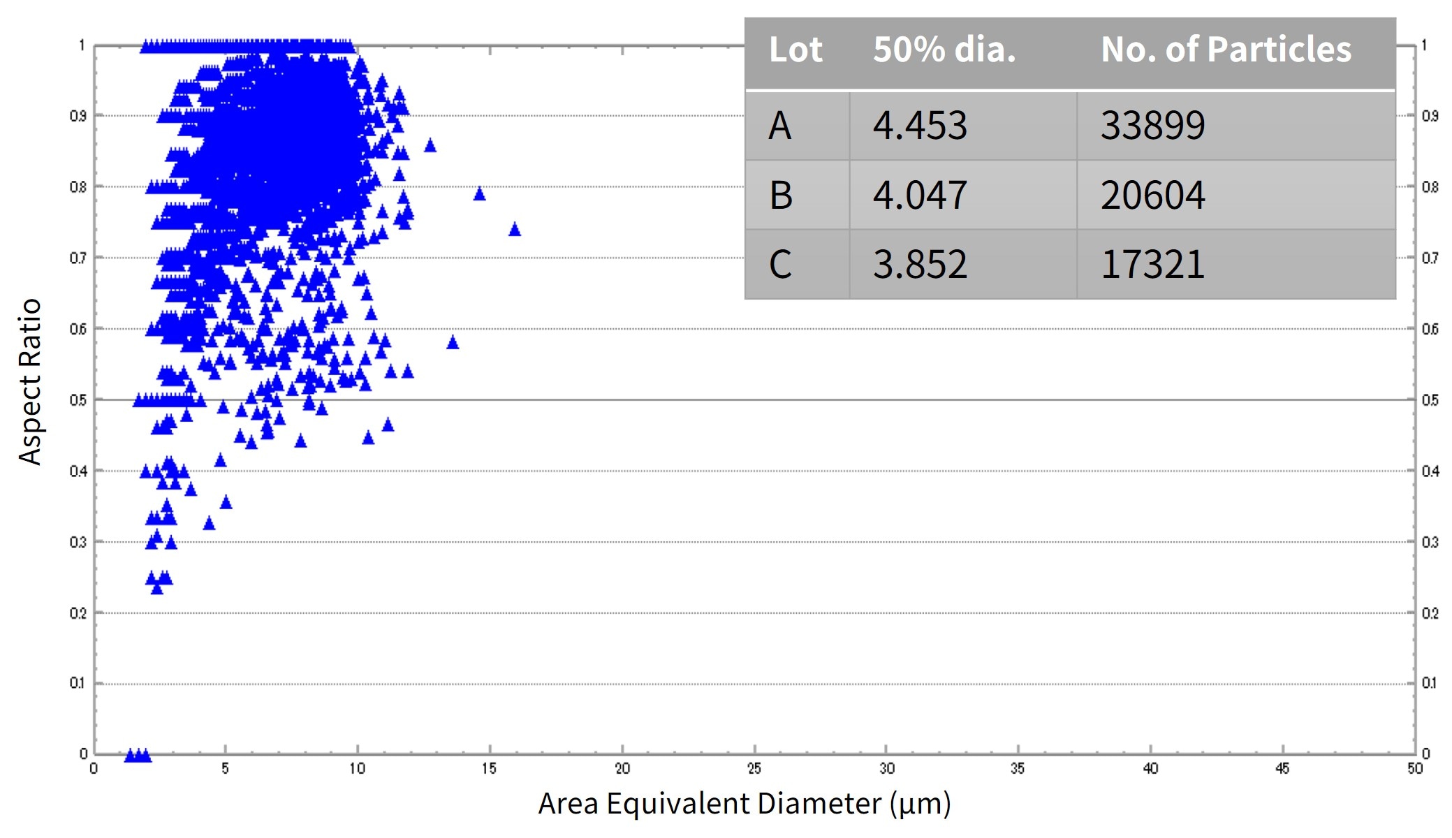
Fig. 4 Evaluation of Particle Sizes in Raw Material Powder Lots
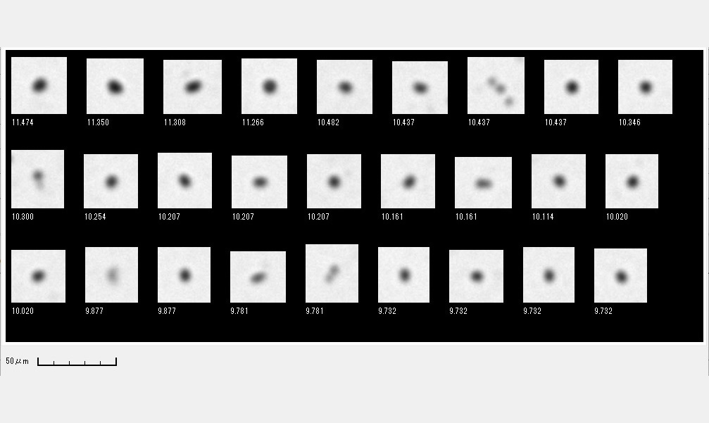
Fig. 5 Particle Images
Related Products
2. Evaluation of Volatile Components
Understanding the components of trace surface treatment agents on silver particles is important for selecting solvents and dispersants used in paste materials prior to sintering. To establish appropriate sintering conditions for silver paste requires determining the volatile components and their thermal properties under various conditions. TG-DTA is effective for measuring the thermal properties and mass changes caused by heating the silver paste, and GC-MS for measuring trace components with high sensitivity.
Measurement Results Using a Thermal Analyzer
Fig. 6 shows the mass change (TG curve) and thermal properties (DTA curve) of a silver paste sample over time during the heating process. The graph shows the temperature and mass at which silver paste volatilizes when heated, along with endothermic reactions occurring around 146 °C and 168 °C. These are used as indicators for selecting raw materials.
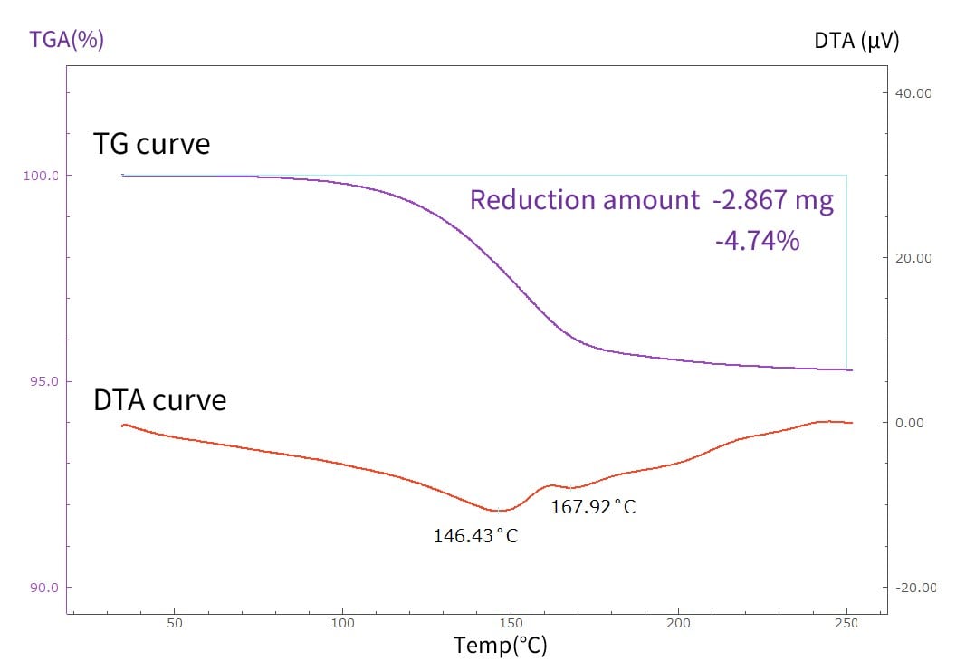
Fig. 6 Thermal Properties and Mass Change of Silver Paste under Temperature Variation
Measurement of Evolved Gas by EGA-MS and GC-MS
Fig. 7 shows the results of measuring the evolved gas when silver paste was heated from 80 °C to 250 °C. Measurements were taken in three temperature ranges: 60-80 °C, 80-150 °C, and 150-250 °C. Fig. 8 shows the TIC chromatograms. As shown, several trace components were detected and characteristic results were obtained for each temperature range.
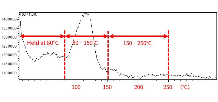
Fig. 7 EGA-MS Analysis Results for Silver Paste
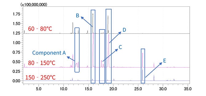
Fig. 8 GCMS Analysis Results for Silver Paste in Each Temperature Range
Related Products

3. Material Strength Properties of Sintered Materials
Power semiconductor modules must exhibit reliable performance against thermal cycling loads and vibration.
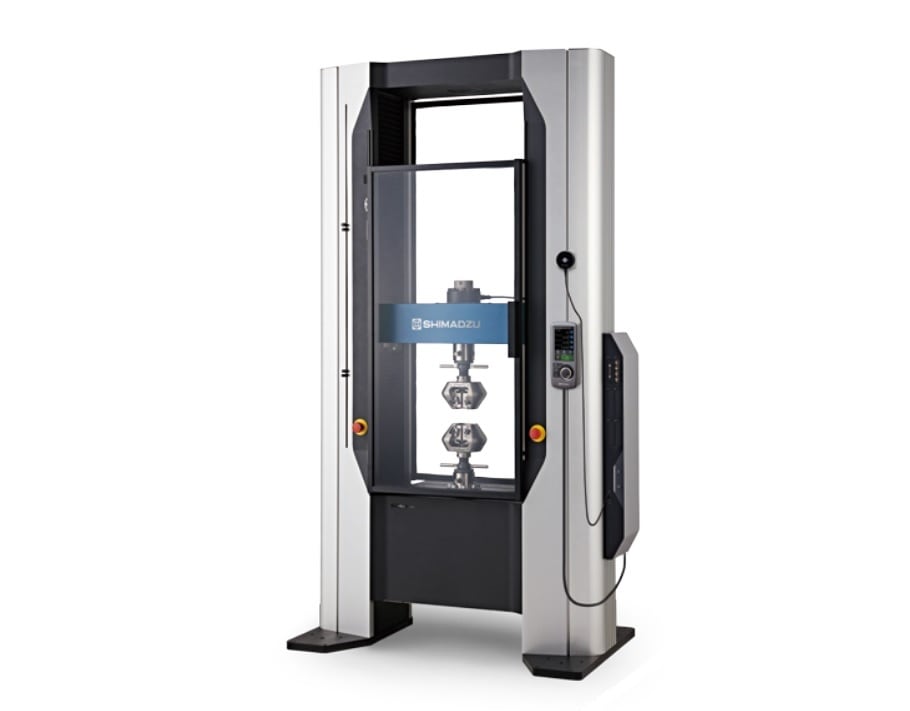
A dynamic fatigue testing machine was used to evaluate the temperature dependence of the strength properties of sintered silver material. Measurements were taken at test temperatures of -55 °C, room temperature, and 175 °C.
The results show that the tensile strength and elastic modulus exhibit an inverse relationship with the environmental temperature.
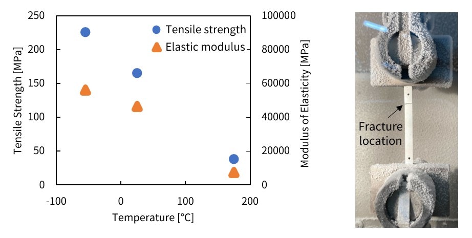
Fig. 9 Strength Property Tests on Silver Sintered Material under Varying Environmental Temperatures
Related Products
4. Shear/Durability Tests and Internal Structure Observation
Static Shear Tests and Durability Tests
Static shear and durability tests on SiC chips are important for evaluating the bond strength. In this example, a static uniaxial shear test was performed on a bonded chip using a special jig. The maximum displacement for the durability test performed under displacement control was set based on the test force-displacement diagram obtained from the static shear test. A cyclic test was conducted using this maximum displacement as the loading condition; failure occurred after 17,988 cycles.
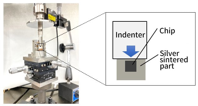
Fig. 10 Special Jig
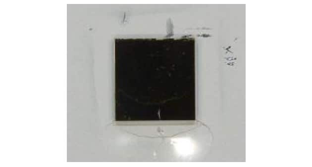
Fig. 11 Photo after the Test (Shear Failure)
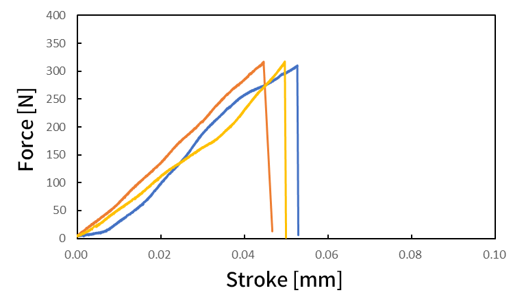
Fig. 12 Example of Results of Static Shear Test
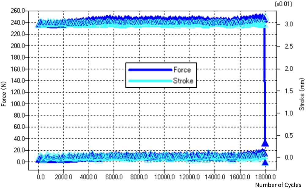
Fig. 13 Graph of Peak Property Values in Durability Test (Failure after 17,988 Cycles)
Non-Destructive Observation with an X-Ray Computed Tomography (CT) System
After the durability tests, the SiC chip failure mode was checked using an X-ray CT system.
Observation clearly and non-destructively confirmed that the silver sintered joint was damaged directly below a damaged area of the SiC chip, and that peeling had occurred on the opposite side to the load direction. This cracking and peeling significantly reduced the thermal conductivity and reliability of the module. For evaluation of internal structures of SiC chips and other parts, non-destructive observation using an X-ray CT system is indispensable.
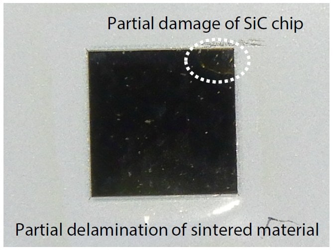
Fig. 14 Test Specimen after the Durability Test
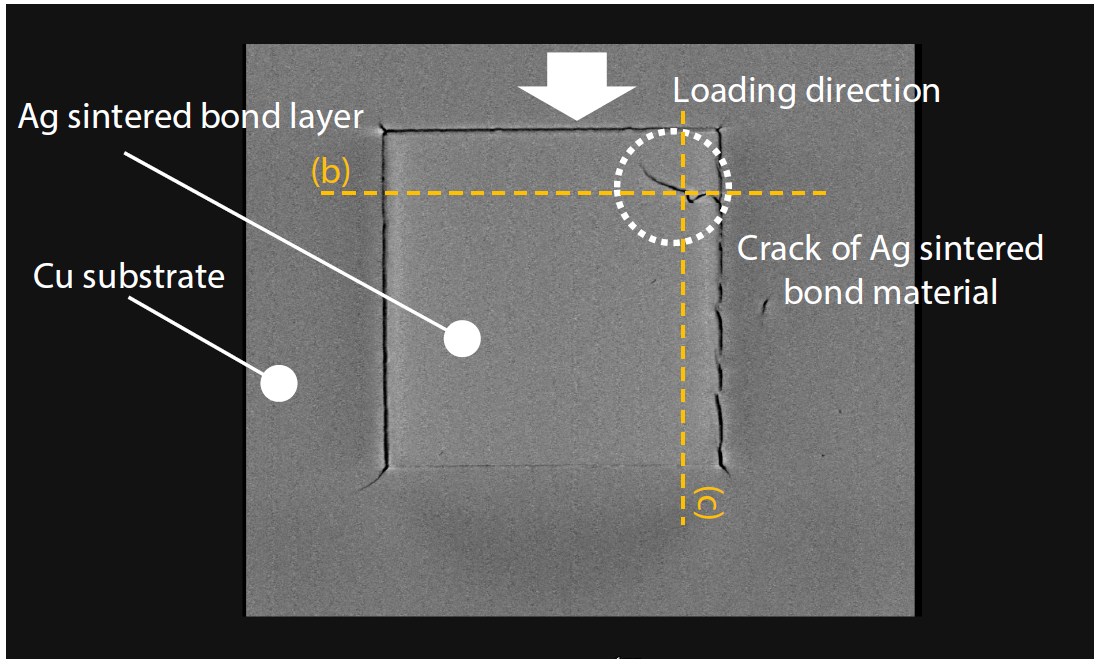
Fig. 15 Cross-Sectional Image of Silver Sintered Joint from above the SiC Chip Surface
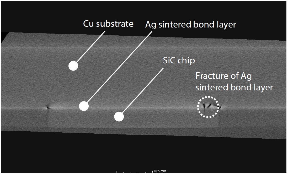
Fig. 16 Cross-Sectional Image from above the SiC Chip Side Surface (Horizontal)
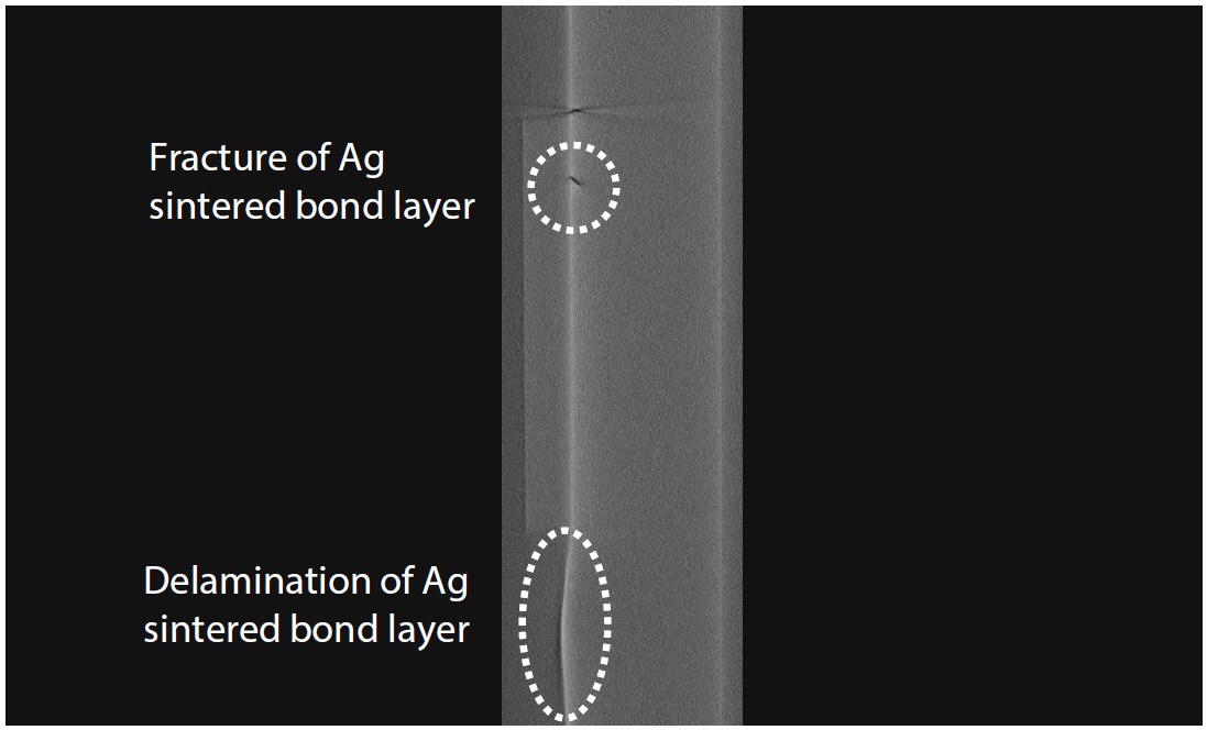
Fig. 17 Cross-Sectional Image from the SiC Chip Side Surface (Vertical)
Related Products

5. SEM Observation/Element Mapping/Analysis of Condition
When evaluating prototypes after a chip has been bonded and when analyzing defects, it is extremely important to check for small voids, map the element distribution, and understand the bonding interface and its chemical bonded state. Introduced here is an example of observation and analysis using an electron probe microanalyzer.
Fig. 18 shows a cross section of the bonded chip. The upper left is an optical microscope image. SEM images (secondary electron images on the left, backscattered electron images on the right) of the chip side, middle, and AMB copper substrate side of the central silver sintered layer were checked. It was confirmed that the condition was virtually uniform and good. Also, areas that appear to be residues of organic components were found in some parts of the prototype (yellow arrow in Fig. 18).
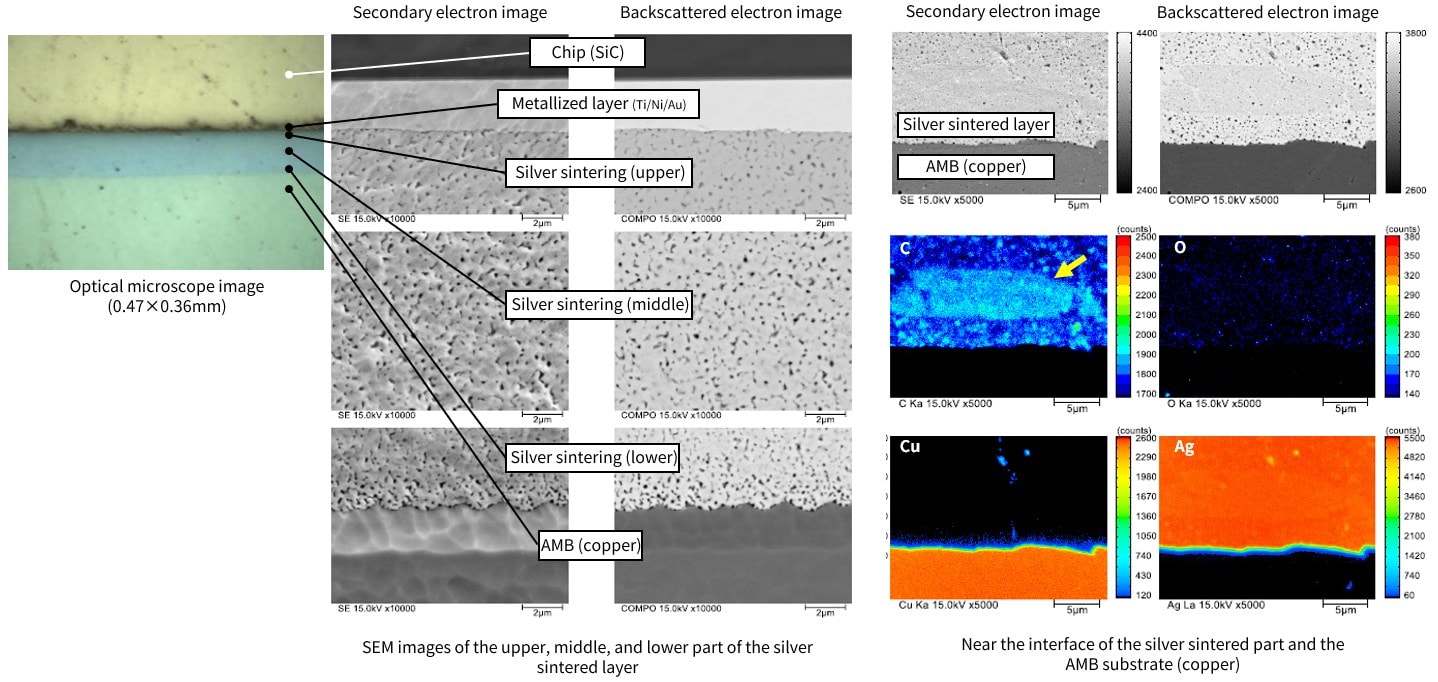
Fig. 18 Observation of Chip Bonding Cross-Section State and Element Mapping Images
By measuring a detailed spectrum of a portion of the peeled surface between the substrate and the chip, we confirmed the oxidation states of Cu on the substrate (the difference between CuO and Cu2O).
When combined with SEM observation, electron probe microanalyzers provide highly reliable analysis of element distribution, composition, and state of even light elements, as well as the chemical bonding state of minute areas (such as differences in oxidation valence), making them effective for determining bonding conditions and performing defect analysis.
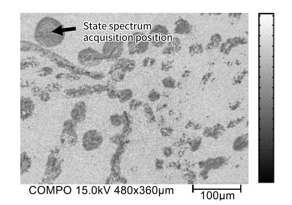
Fig. 19 Backscattered Electron Image of the Peeled Surface
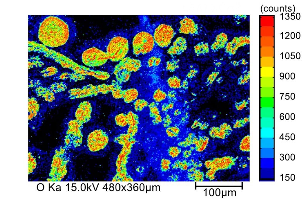
Fig. 20 Element Distribution on the Peeled Surface (O)
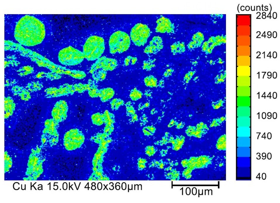
Fig. 21 Element Distribution on the Peeled Surface (Cu)
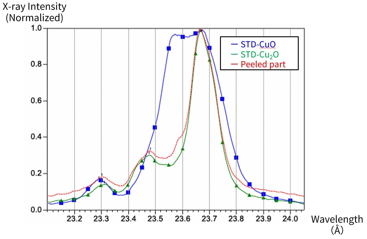
Fig. 22 State Spectrum of the Peeled Part
(In the legend, STD refers to the standard sample)