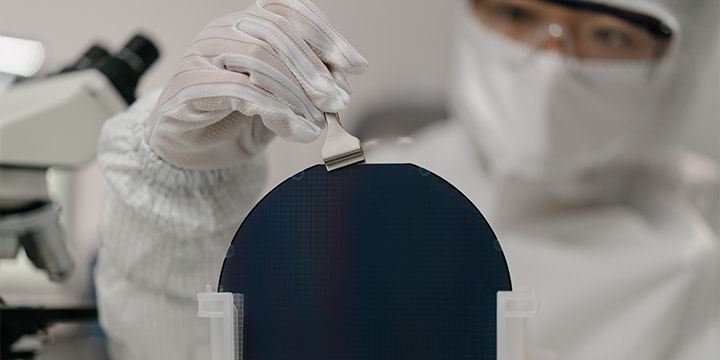
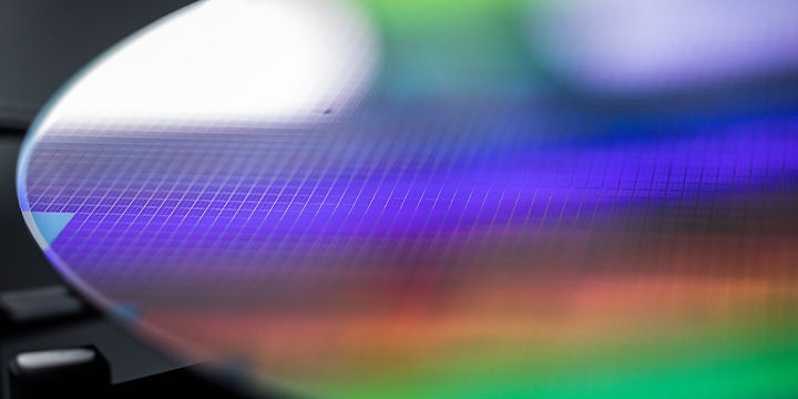
Wafer
Evaluation of Manufacturing Processes
Semiconductor devices are manufactured through a series of processes that begin with wafer fabrication, followed by repeated steps of cleaning, polishing, deposition, lithographic exposure, development, and etching. The process ends with dicing, bonding, and molding.
It is understood that semiconductor manufacturing involves repeating the above processes about several hundred to a thousand times, and it is vital not to pass defective wafers to the next step. Therefore, inspections during each process and management of materials used in each step are necessary. Here, we introduce various analysis examples for each process step.
-
-
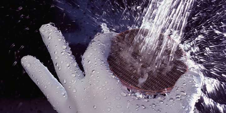
Lithographic Exposure/Development
-
-
-
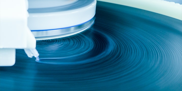
Planarization in the Polishing Process
-
-
Instruments Used for Evaluation
Listed here are the major evaluations required in the manufacturing process and the instruments used to perform them.
| Manufacturing Process | Major Evaluation | Details | Instrument |
|---|---|---|---|
| Wafer manufacturing | Surface inspection | Evaluation of surface roughness and electrical characteristics | SPM |
| Qualitative and quantitative analysis of elements and analysis of chemical bonding states | XPS | ||
| Non-destructive testing | Observation of voids and etch pits at resin interfaces | Microfocus X-Ray | |
| Contaminant inspection | Evaluation of micro-contaminants | FTIR / Raman | |
| High-speed imaging | Evaluation of failure process | HPV | |
| Lithographic exposure and development | Optical properties | Evaluation of photosensitivity, uniformity, and film thickness | UV |
| Surface inspection | Evaluation of resist film irregularities, roughness, and uniformity | SPM | |
| Composition analysis | Composition analysis of chemically amplified resists and base resin copolymerization | LCMS | |
| Confirmation of synthesis of low molecular weight compounds and impurity analysis | GCMS | ||
| Etching and deposition | Gas analysis | Analysis of impurities and organic compounds | GC, GCMS |
| Evaluation of trace components in process gases | FTIR (Gas Cell) | ||
| Surface inspection | Observation of fine structures after etching | SPM | |
| High-speed imaging | Observation of plasma behavior during etching | HPV | |
| Cleaning | Contaminant inspection | Inspection of trace organic residues and impurities remaining on the wafer surface | UV |
| Liquid analysis | Composition analysis | HPLC | |
| Total organic carbon analysis | Management of wastewater, pure water, and ultrapure water | TOC | |
| Planarization | Particle size distribution | Evaluation of coarse particles in abrasives and CMP slurries | DIA |
| Nanoparticle evaluation using laser diffraction and scattering analysis | SALD | ||
| Separation and detection of large particles, emulsion fractionation analysis | FFF (Centrifugal Field-Flow Fractionation) | ||
| Composition analysis | Identification of trace components and impurities in CMP slurries | LCMS | |
| Analysis of the polymeric structure of surfactants | MALDI | ||
| Microcompression testing | Evaluation of abrasive hardness, elastic modulus, and plastic deformation properties | MCT | |
| Electrode formation | Liquid analysis | Analysis of additives in plating solutions | HPLC |
| Management of inorganic substances in plating solutions | AA, ICP | ||
| Quantitative analysis of siloxanes | LCMS, GCMS | ||
| Dicing | Physical property testing | Adhesion testing of dicing tape, etc. | Autograph |
| Bonding | Composition analysis | Analysis of halogens in resins | HPLC (Ion Chromatograph) |
| Physical property testing | Tensile strength test of ultra-fine metal wires | Autograph |